General Specification for HDI PCB
Layer Count: 4-20Layers
Type of stack up: 1+N+1, 2+N+2
Material Available: FR4, High Tg FR4, Halogen Free FR4
Board thickness: 0.4-3.2mm
Finished copper thickness: 1/3oz ®C 3oz
Min trace width/spacing: 3/3mil
Min through hole: 0.2mm
Min blind via: 0.1mm
Surface treatment: Immersion Gold, ENIG + OSP
==============================================
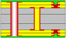
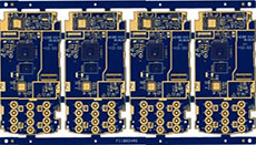
High-density interconnection/HDI PCB
Layer: 6(HDI)
Structure: 1+4+1
Material: FR4
Thickness: 0.8mm
Min trace width/spacing: 0.076/0.076mm(3/3mil)
Surface treatment; Immersion Gold
Blind via L1-2 & L5-6: 0.1mm(4mil)
Buried via L2-5: 0.2mm(8mil)
Application: telecommunication
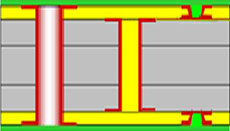
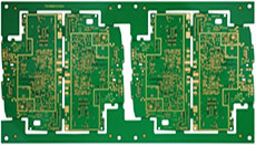
High-density interconnection/HDI PCB
Layer: 8(HDI)
Structure: 2+4+2 with stagger via
Material: FR4£®Halogen free)
Thickness: 1.0mm
Surface treatment; Immersion Gold
Blind via L1-2 & L2-3 & L6-7 & L7-8: 0.1mm(4mil)
Buried via L3-6: 0.2mm(8mil)
Impedance control: differential 90 & 100ohm
Application: telecommunication
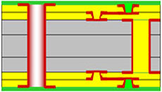
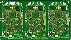
High-density interconnection/HDI PCB
Layer: 8(HDI)
Structure: 2+4+2 with stack via
Material: FR4(Tg170)
Thickness: 1.0mm
Surface treatment; Selective Immersion Gold + OSP
Blind via L1-2 & L2-3 & L6-7 & L7-8: 0.1mm(4mil)
Buried via L3-6: 0.2mm(8mil)
Special process: Copper-filled on L2-3 & L6-7
Application: telecommunication
